Investigation of Photonic Structure
Within the last decade the research field of Optoelectronics and Photonics has emerged as an active and successful focal area at the Paderborn University. Some highlights investigated are novel light diodes & lasers, ultrafast digital communication via fibers, integrated optical circuits, biological photonic structures, concepts for optical quantum computers, optical sensors, antennae for light, metamaterials, and holograms from ultrathin layers.
The fundamental interplay of light and matter in nanostructures has been investigated at the Paderborn University for a long time. In addition to the many individual projects and bilateral cooperations, several large-scale joint projects have resulted since the “Center for Optoelectronics and Photonics Paderborn (CeOPP)” was established in 2006. In 2008, a DFG graduateschool involving 15 research groups and 26 PhD students working on the topic of “Micro- and Nanostructures in Optoelectronics and Photonics” began, and established in 2013 a DFG SFB/Transregio on “Tailored nonlinear photonics: From fundamental concepts to functional structures” together with TU Dortmund.
Embedded into this fruitful research environment, Professor Jens Förstner’s group, uses theoretical models and numerical simulations to investigate photonic structures, often in close collaboration with the many world-class experimental groups at Paderborn University and external partners.
This article is a reprint of an article which has previously appeared in the research report 2014–16 of the Paderborn Center for Parallel Computing. Please refer to the complete research report for additional information about our institution further articles on projects enabled by our HPC infrastructure.
THE FUNDAMENTALS OF LIGHT IN PHOTONICS
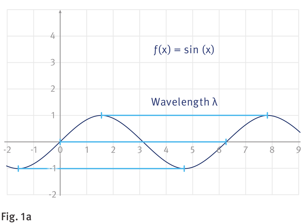
The previously described effects and applications of photonics are based on the fact that light is an electromagnetic wave. The fundamental idea can be illustrated using a familiar form of waves, such as water waves. From those we can see that a wave oscillates in time while traveling through space. But where a water wave requires liquid as medium, electromagnetic waves travel freely through space – instead of the medium, the electric and magnetic fields oscillate. A key quantifier of waves is wavelength, which measures the distance from one wave maximum to the next (see Figure 1 a). For water waves, the wavelength ranges from centimeters to few hundreds of meters. Electromagnetic waves also exist at these wavelengths – those are the radio waves as known from radio/tv broadcasting, radar, wi-fi or mobile phones. But only if the wavelength of electromagnetic waves is much smaller – about onemillionth of a meter – they trigger signals in the receptors of the human retina, which enables us to see, and are known as visible light.
Exactly as water waves scatter and reflect off stones, bridges, and shores, in photonics one can utilize different materials to scatter and reflect light waves. One interesting property is that waves coming from two directions can both constructively and deconstructively interfere with each other. While this interference is rarely exploited for water waves, it is often utilized in photonics to radiate light into a certain direction, to guide it onto a particular molecule, to focus it into a desired area, or to direct it towards an optical sensor. To make optimal use of this interference effect, however, the structures must have features smaller than the optical wavelength i.e., the range of few nanometers – used today in modern lithography equipment such as that available in Paderborn’s CeOPP center.
Additionally, the range of possibilities extends beyond the geometry and also to the type of material that can be varied. For example, for some materials light travels faster than in others, and in the case of metals, light sticks to the surface and is partially converted to heat. And in so-called nonlinear materials, the oscillation frequency, and with it, the color of the light can be converted – which is quite handy if one only has a red light diode but needs green light.
All these effects, ranging from the interference of electromagnetic waves to material properties, are mapped to problem-specific models addressed by the group of Jens Förstner using physical equations. The variety of materials and geometries within one simulation leads to large and complex systems of equations requiring numerical evaluation. For this, the structures and the surrounding space is decomposed into many small spatial elements, which are then stored and processed in a computer. But often many elements are necessary that cannot completely fit into the memory of a single computer. Here, PC² comes into play.
Our model is distributed onto dozens to hundreds of computers, each storing and computing only a small part of the full space. However, since light travels between these parts, the computers have to exchange the relevant information – and therein lies the strength of high-performance computing centers like the PC² with their special and fast network interfaces.
The figures show examples for structures investigated by Förstner’s group. First, Fig. 2 illustrates a structure optimized to capture light from outside and to focus it into a small area (i.e., on the order of an embedded molecule). To achieve the best possible light concentration over 1,000 different models with a systematic variation of parameters, were simulated on the PC² computer cluster. The shown geometry performs several times better compared to existing solutions.
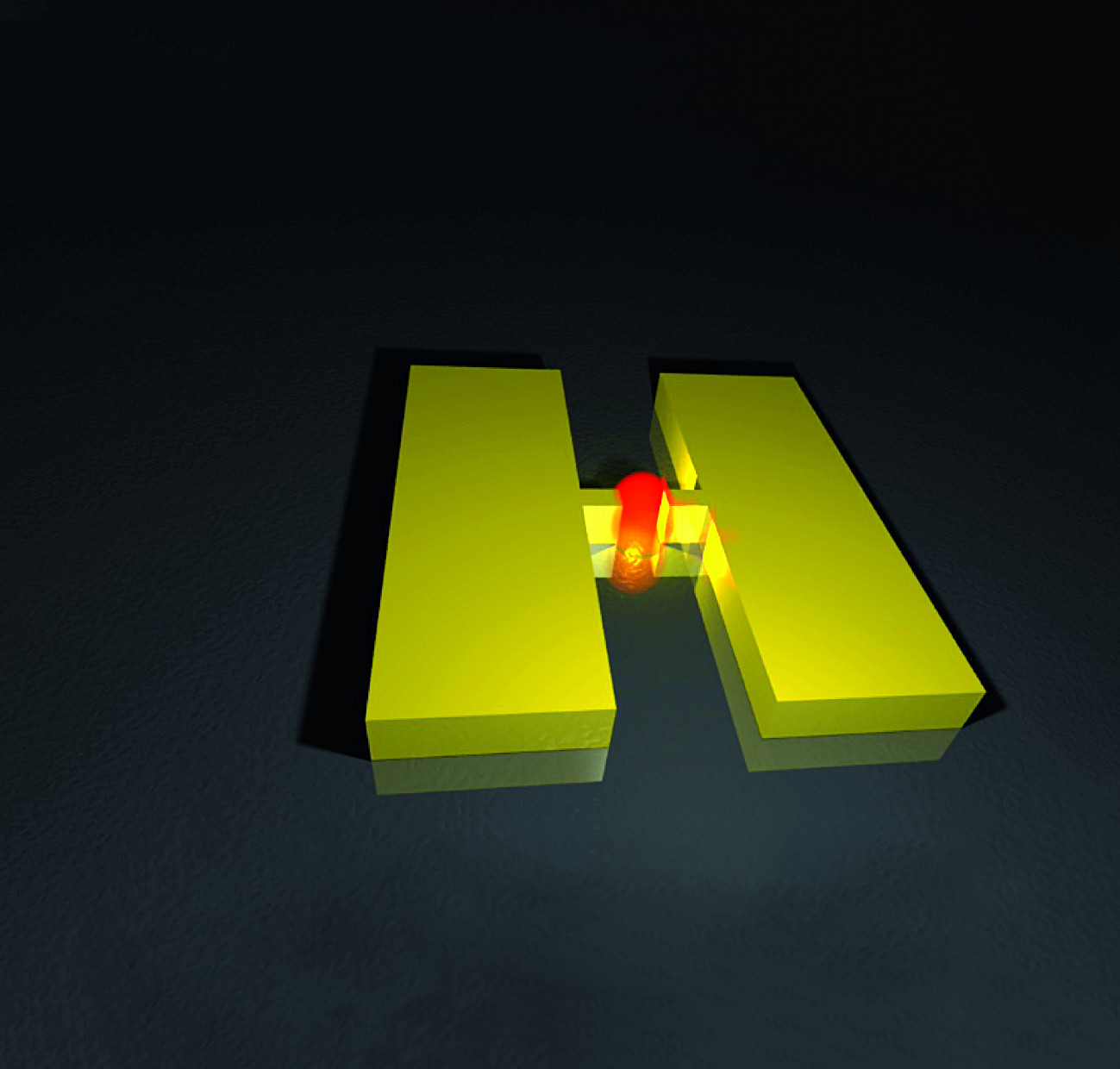
The structure in Fig. 3 represents an optical antenna – a miniaturization of a radio-frequency roof antenna to the nanoscale making it suitable for optical light. By using simulations on the PC² cluster it was possible to show that the proposed structure has a better directional characteristic compared to existing optical antennas. Although the calculations have only recently been finalized, there are already experimental results from co-workers which confirm the efficiency of the design. With this work, a wide spectrum of other photonic structures has been investigated by Förstner’s group including metamaterials, photonic crystals, quantum dots, integrated waveguides, biological structures – and even interplanetary dust.
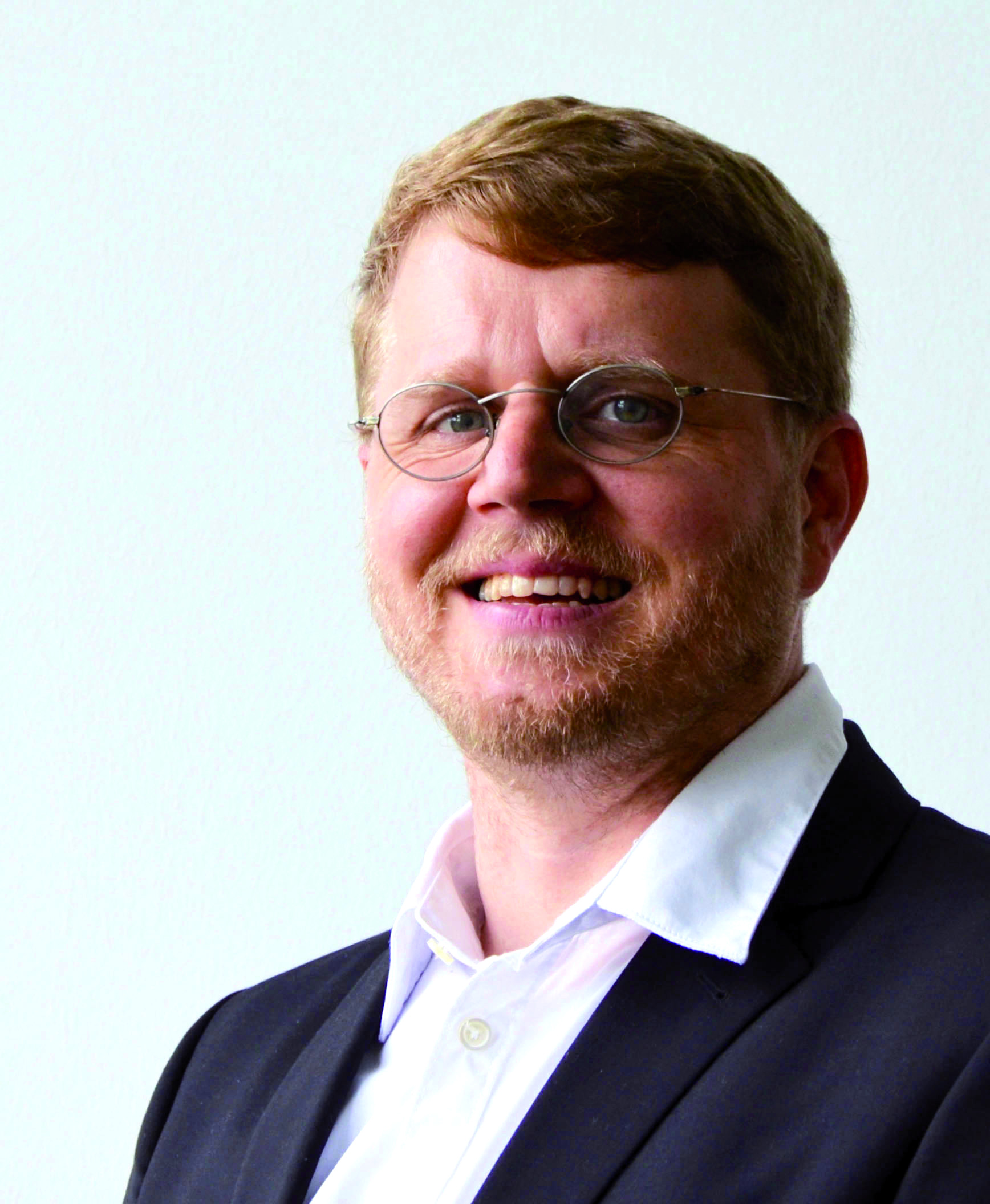
Prof. Dr. Jens Förstner
Jens Förstner, head of the Theoretical Electrical Engineering (TET) group at Paderborn University, studied Physics and Computer Science at Philipps Universität Marburg and University of Kent at Canterbury/UK. During his PhD at Technical University Berlin and later for postdoctoral studies at University of Arizona, where he focused on simulating nanophotonic structures, Förstner led an Emmy Noether research group on “Computational Nanophotonics” in Germany and was appointed full professor in 2013.
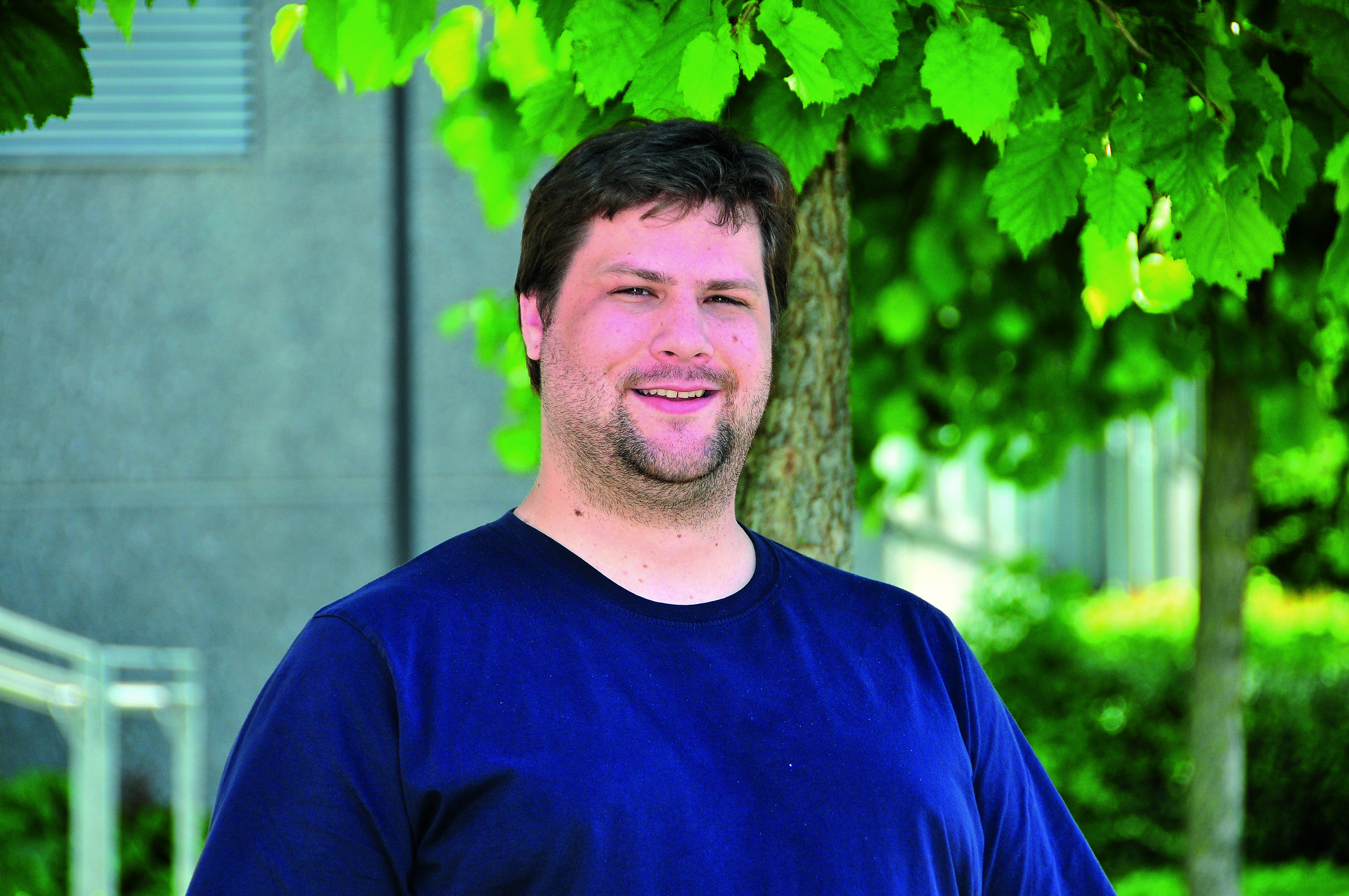
Dr. André Hildebrandt
André Hildebrandt recently completed his PhD in the Prof. Förstner’s research group in the area of “Micro- and Nanostructures in Optoelectronics & Photonics”. His research focus is on applied and integrated Optics and Numerics. Previously, he has been working for the automotive company Hella KG for several years after graduating from Paderborn University with his Master’s thesis “Numerical Simulation of light coupling into photonic crystal defect wave guide”.


